
Research in the Nguyen Group focuses on organic electronic devices, such as photovoltaics, photodetectors, and electrochemical transistors. We characterize devices and the organic, semiconducting materials utilized in these devices by a variety of electrical, optical, and structural measurements to elucidate the influence of chemical structure on the properties and performance of devices. With an ever-evolving understanding of the underlying mechanisms that govern device performance, we can design new materials, processes, and device architectures to progress this field toward commercially viable, light-weight, and flexible organic electronics.
Organic Electronics
- Organic Photovoltaic Devices
- Charge Transport & Charge Recombination
- Morphological Characterization
- Interfaces in Organic optoelectronics
- Organic Photodetectors
- Organic Electrochemical Transistors(OECTs)
- Conjugated Polyelectrolytes (CPEs)
- Organic Field-Effect Transistors (OFETs)
- Electron Transport in Biofilms
- Organic Electronic Devices for Tactile Sensing Applications
- Novel doping of Organic Semiconductors
- Exciton Diffusion in Organic Semiconductors
Organic Photovoltaics

A bulk heterojunction organic photovoltaic (BHJ OPV) device consists of a ~100 nm thick film comprising a blend of an electron donating and electron accepting material that phase segregate to form nanoscale, bicontinuous domains. Upon exposure to light, a photon absorbed by one of the materials promotes an electron from its highest occupied molecular orbital (HOMO) to its lowest unoccupied molecular orbital (LUMO), creating a bound electron–hole pair known as an exciton. This exciton can diffuse within the film and may reach an interface between the electron donor and electron acceptor. At this interface, there is an energetic driving force for the exciton to split into free charges, with the electron in the acceptor and the hole in donor. Once charges are formed, an electric field created by two electrodes of differing work functions provides a driving force to sweep out the generated charges, with the electrons travelling through the acceptor domains to the cathode and the holes travelling through the donor domains to the anode.

For our studies, we fabricate small solar cells on glass substrates that contain a transparent conductive material, indium tin oxide. We first add a transparent conductive polymer, which serves as one electrode, then cast our organic semiconductor blend from a single solution via spin-coating. The two materials phase separate into an interconnected network of donor and acceptor phases upon drying by evaporation of the solvent, which, as mentioned above, strongly influences the performance of OPV devices. We work to control the nanoscale morphology of the blend film by adjusting the parameters of our organic film processes, including the solvents, solvent additives, concentration, blend ratio, spin rate, and temperature. A low work function, reflective metal contact is then added to the top surface via thermal evaporation through a shadow mask. The end result is an organic film sandwiched between two electrodes. To test the cells, we use a lamp that mimics the spectrum and intensity of sunlight, and measure the current generated as a function of voltage. Comparing the maximum power generated to the total power available from the incident light gives an efficiency value.
We study in depth the photo-physical processes in the devices by applying a wide range of materials and device characterization techniques, such as solid-state NMR, capacitance spectroscopy, UV/Vis spectroscopy, FT-IR, JV curve measurements, atomic force microscopy and external quantum efficiency measurements and optical simulations. We use these tools to understand the origins of the OPV performance and to find new ways of obtaining OPVs with higher efficiency, increased lifetime or reduced environmental impact.
Semitransparent OPVs

One of our current fields of interests are (semi)transparent OPVs (ST-OPVs) for integrated energy harvesting. ST-OPVs can be integrated into windows to harvest energy on-site, allowing unlimited architectural design possibilities and natural lighting for buildings. When integrated into greenhouses, they can generate electricity while selectively transmitting the spectral range necessary for unhindered plant growth. To meet the requirements for semitransparency, the active layer of the solar cell must absorb light outside the visible range (380–780 nm) while maintaining high transparency in the visible range. The emergence of versatile non-fullerene acceptor (NFA) molecules for BHJ solar cells played a leading role in the development of ultra-narrow bandgap systems. These have paved the way for the desired high absorption in the infrared range that is accompanied by a high average visible transmittance (AVT). Our studies have focus on inherent changes in the device physics and resulting recommendations, as well as on approaches to increase the transparency of the OPVs.\
Green-solvent Processing OPVs

Our group is also interested in developing organic semiconductors with molecular structures tailored for solubility in “green solvents” and efficient transport of charge carriers in the solid state. Organic semiconductors have been widely applied into organic solar cells (OSCs), wearable electronics and organic photodetectors (OPDs) in the last decades for their lightweight, flexibility and great industry potential for high throughput solution processing and roll-to-roll printing technologies. However, traditional solvents used for these organic photovoltaics processing conditions are commonly highly toxic halogenated organic solvents like chlorobenzene (CB), o-dichlorobenzene (o-DCB), tri-chlorobenzene (TCB) and chloroform (CF), which are not only harmful to human health upon exposure but can also cause long-term effects on ecosystem. Consequently, research on halogen-free/ “green solvent” (such as xylene, 2-methyltetrahydrofuran (2-MeTHF), methanol, water, etc.) processable organic semiconductors is essential to moving organic photovoltaics from bench chemistry towards real-life applications.
As shown in the figure above, we have developed a PPDT2FBT:PC61BM bulk-heterojunction (BHJ) system processed from a green solvent, ortho-xylene (o-XY), which is investigated in comparison with the same blend processed from a traditional halogenated solvent, chlorobenzene (CB). The BHJ blends are characterized with various techniques probing at difference length scales, and an increased donor:acceptor (D:A) interfacial area as well as well-mixed features in the bulk morphologies of the active layer are observed for the o-XY processed BHJ blend. Furthermore, molecular-level differences in the D-A intermolecular interactions at the BHJ interfaces in o-XY and CB cast films are elucidated by 2-dimensional solid-state nuclear magnetic resonance (ssNMR) measurements and analysis. These results are consistent with the device properties, suggesting that the green-solvent-processed devices have longer charge carrier lifetimes and faster charge carrier extraction. The optimized PPDT2FBT:PC61BM devices processed from o-XY can achieve a noteworthy higher power conversion efficiency (PCE) owing to a higher short-circuit current density and fill factor.
Charge Transport and Charge Recombination
Charge carrier transport and carrier recombination govern the operation of all electronic devices, including those utilizing organic semiconductors. Thus, understanding charge transport and charge recombination in organic semiconductors is a prerequisite for successfully designing future high performance organic electronic devices such as solar cells, field-effect transistors or light emitting diodes.
In our group, we study charge carrier transport by fabricating field-effect transistors and (single-carrier) diodes. Understanding the energetics of the organic materials allows us to isolate either hole or electron transport by choosing electrode materials with the correct work functions relative to the frontier energy levels of a given organic compound. Analysis of the current–voltage characteristics of these devices provides information about how fast these charge carriers are transported through the organic material in the precence of an applied electric field, which is known as their mobility. Furthermore, with an understanding of the mobility’s dependence on temperature, we can get information about the width of the density of states (DOS) and the activation energy (Ea) in the organic semiconductor systems. By characterizing mobility values in pristine donor/acceptor materials and blends, we can not only understand the underlying mechanisms that dictate device performances, but also provide insights on the design and synthesis of new and improved materials.

We employ a variety of techniques to understand the recombination mechanisms in organic semiconductors. Studying double carrier devices enables us to investigate the process of holes recombining with electrons. This process is a fundamental loss mechanism in organic solar cells, but is essential to the operation of light emitting diodes. Additionally, we probe recombination mechanisms by looking at the photoluminescence, electroluminescence, quantum efficiency, and impedance response of organic electronic devices as a function of temperature and excitation energy.
Morphological Characterization
The performance of organic electronic devices is profoundly influenced by the nanoscale morphology of the organic film. For example, the active layer of a bulk heterojunction organic photovoltaic (BHJ OPV) device is a ~100 nm thick film consisting of a blend of an electron donating and electron accepting material that phase segregates to form nanoscale, bicontinuous domains. The size, purity, order, and distribution of these nanoscale domains all affect each of the processes that govern solar cell efficiency. Therefore, having control over nanoscale morphology is of great importance.

Given the complicated nature of organic thin films, no one technique can fully describe the nanoscale morphology. In order to probe the nanoscale morphology of organic films, we employ a variety of different characterization techniques. By utilizing a variety of different techniques, we can more completely describe a given system in order to develop structure-property-processing relationships that will guide the development of future materials and devices. By comparing the nanoscale morphology of related OPV systems that perform differently, we can identify morphological characteristics that either help or hurt device performance, and then tune our fabrication procedures accordingly. The figure below is an example of how the nanoscale morphology of an organic film (in this case a small molecule donor:fullernene acceptor BHJ OPV) can be studied with several different techniques, which each provide unique structural information about the system.

Interfaces in Organic Optoelectronics
The operation of organic electronic devices strongly depends on the charge injection or charge extraction properties of the metal contact. The interfaces between metal electrodes and organic semiconducting materials play a crucial role in these processes. The graphs (from left to right) below illustrate device architectures of organic light-emitting diodes (OLEDs), solar cells (OPVs) and field-effect transistors (OFETs), respectively. Generally speaking, good energetic alignment between the electrode work function (WF) and the conduction (valence) band of the electron (hole) conducting material is desired to maximize device performance. At the same time, the unique requirements of each application (photovoltaics, light-emitting diodes, and field-effect transistors) limit the range of suitable electrodes. For example, to produce electroluminescence in the PLED (left graph), electrons have to be injected from the top cathode to recombine with holes injected from the bottom anode. An opposite process occurs in the OPV (middle graph) where charges created in the active layer must be extracted at the electrodes to result in the photoconductivity. In the OFET (right graph), the current is formed via charges injected from the source electrode under the modulation of gate bias. In OLEDs and n-type or ambipolar FETs, for instance, efficient injection of electrons from a metal electrode to the LUMO of the organic material is necessary. A reactive, low WF metal electrode provides a suitable contact to the LUMO of organic materials but simultaneously raises a problem of air stability. Thus it is favorable to have stable materials with tunable WFs so that charge injection can be preferentially improved without complicating the device structure and fabrication procedure. An emerging alternative to a low WF metal is a solution processable interlayer between the organic film and the metal electrode that effectively modifies the electrode work function while maintaining its otherwise desirable characteristics such as stability and cost.
In reality, the charge injection efficiency is often limited by the choice of metal electrodes, undesirably affecting the ultimate device performance. To circumvent this shortage, interlayers are introduced to deal with charge injection issues. For instance, interlayers consisting of a thin organic film or DNA film have been incorporated in OLEDs, OFETs, or OPVs from solution processing. As a result the work function of the top electrodes is modified such that charge injection barriers are effectively reduced. This modification leads to improving the luminance efficiency (in the case of OLEDs) and charge carrier mobility in OFETs. To understand the impact of interlayers on the device performance, we employ a combination of techniques including ultraviolet photoemission spectroscopy (UPS), X-ray photoemission spectroscopy (XPS), AFM, (scanning) Kelvin probe microscopy, electrostatic force microscopy, conducting AFM and contact angle measurements, etc. From these measurements, we aim to attain insights into the interfacial properties at the metal/organic interface.

Organic Photodetectors (OPDs)

Sensitive detection of visible and near-infrared (NIR) light enables many important applications in both research and industry. Our group has developed several high-performance solution-processed BHJ OPDs based on a new ultranarrow-bandgap nonfullerene acceptor, whose photosensing performances are on par or surpass those of conventional Si detectors. In addition, we have developed highly sensitive photomultiplication (PMT) OPDs, which exhibit broadband spectral activity from the ultraviolet and visible region to the infrared region, low operating voltage, and fast response.
We are currently pursuing to bridge the knowledge gap between the laboratory-prototype OPD and a real product. We study in depth the thermal stability, photostability and long-term stability in the OPD, which are extremely crucial for the implementation of this photosensing platform in readout integrated circuit (ROIC) and photonic integrated circuit. On the other hand, we are greatly interested in material design for high performance active layers and interlayers for ultra-high detectivity OPDs, with large photosensing area and flexibility.
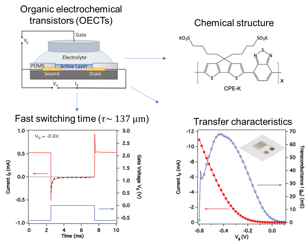
Organic Electrchemical Transistors (OECTs)
Organic electrochemical transistors (OECTs) have attracted tremendous attention in research and engineering communities because of their unique features, which are well suited to biomedical applications, and consequently have led to their growing use in many areas of biomedical engineering The main components of an are the source, drain, and gate electrodes, an organic semiconductor channel connecting the source and the drain, and an electrolyte that interfaces with both the gate and the semiconductor. The electronic current from the source to the drain electrode can be modulated via ion migration from the electrolyte to the channel, causing doping/dedoping electrochemical reactions of the organic semiconductor. Such ion migration requires a low gate voltage (∼1 V). The channel conductance in these devices is generally high, and, as a consequence, the operating voltage of an OECT can be considerably smaller than is required in organic field-effect transistors. Moreover, OECTs can operate robustly in ambient air and variable humidity and utilize components made from biocompatible materials or even naturally occurring materials.
OECT projects in Nguyen’s group focus on three fronts: developing new materials for OECTs, investigating device physics of OECTs with new fabrication techniques and device structure, and demonstrate applications of OECTs in electronics and in chemical/biosensing. Some selected past and ongoing projects are:
Conjugated Polymer Electrolytes (CPEs) for OECTs
A self-doped CPE material was utilized to fabricate high transconductance accumulation mode OECTs (figure below). The direct cross-linking of GOPS to the sulfonate functional group on CPE-K was demonstrated by XPS. OECT devices fabricated with CPE-K exhibited accumulation mode opera- tion, which allows for low power consumption as the device is usually in the OFF state. The transconductance of OECTs made from CPE-K was compared to other OECT materials reported in the literature by considering device channel volume and operational voltage. In addition, CPE-K-based OECTs show rapid switching times and stability over the range of temperatures relevant for biological applications. CPE-K demonstrates volu- metric capacitance under an applied positive DC bias, which is consistent with the movement of ions made possible by their compensation from polarons in CPE-K. The volumetric capacitance of CPE-K was 130 C cm-3, demonstrated using impedance spectroscopy on films of varying thicknesses and the calculated capacitance per square unit of CPE-K was confirmed with gate transient measurements. This result highlights the potential of conjugated polyelectrolytes in OECTs and point toward future designs of CPEs for use in OECTs. A wide range of high mobility D–A conjugated back- bones have been discovered by the OFET community, and can be adapted for use in OECTs by utilizing water soluble sidechains such as sulfonate functional groups. CPE-K ranks among the highest performing materials for accumulation mode OECTs and represents a shift away from PEDOT:PSS toward a more widespread use of novel materials in organic electrochemical transistors.
Biomaterials as the solid electrolyte model to unveil the protonic doping and dedoping in OECTs
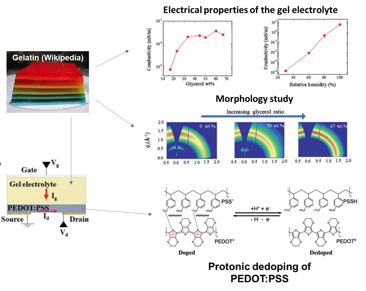
We investigated in-depth study of biomaterial- based solid-state OECTs in which gelatin-glycerol biogels were employed as a model solid electrolyte because of their excel- lent processability and ion-conductivity. The ion-conductivity of the gels was made as high as 6.02 mS m−1, and their morphology/conductivity relationship was investigated. Adding of glycerol in gelatin suppresses ordering in the gelatin-glycerol gels, which eliminates the lamellar stacking and hence contributes to the rise of conductivity in the direction perpendicular to the substrate. A temperature-dependent characterization of the biogel OECTs indicated the exclusive role of protons in the electrochemical doping/ dedoping of PEDOT:PSS, based on which the working principle of the biogel OECTs was proposed. As a soft-material, gelatin-glycerol gels allow the fabrication of conformable and biocompatible electronics components and devices, which are prerequisites for good wearable and implantable electronics.] All materials used in this study are commercially available in large quantity and low cost, making it possible for other research groups to adopt these architectures to their custom needs, accelerating the implementation of soft electronics in domains such as neural implants or electronic skins.
New efficient fabrication technique via wet-chemical processing
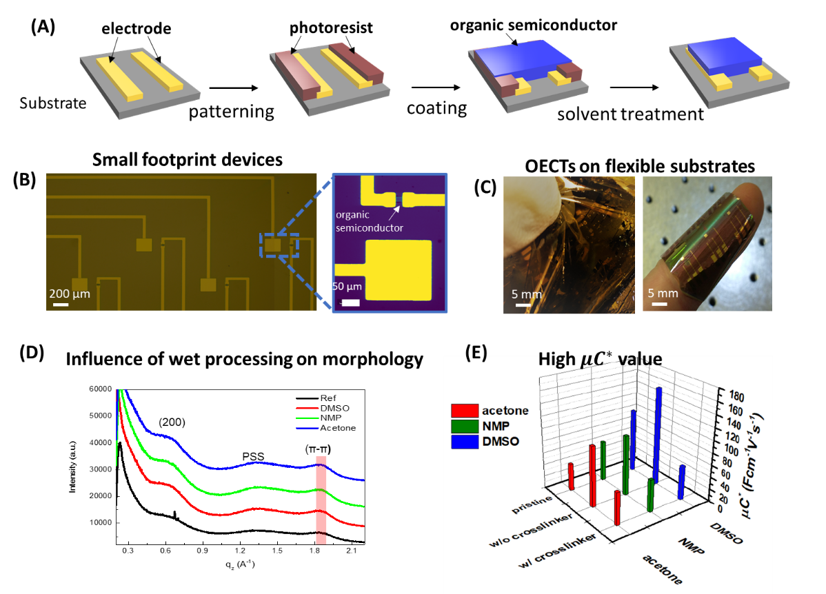
Currently sophisticated and expensive state-of-the-art fabrication techniques and processes represent a barrier in OECT research, therefore limiting new experimental investigation of these transistors for broader applications. in the quest for simpler OECT fabrication techniques, the use of wet chemistry based on polar solvents has been left out because it is believed that this would result in detrimental effects on the active materials. At the same time, some organic solvents, such as dimethyl sulfoxide (DMSO) were shown to enhance the performance of OECTs based on PEDOT:PSS. Moreover, PEDOT:PSS used in OECTs requires crosslinkers such as (3-glycidyloxypropyl) trimethoxysilane (GPOS) for stabilization, and the effect of polar solvents on the performance of crosslinked PEDOT:PSS-based OECTs has not been reported. We exploited these avenues to demonstrate an efficient fabrication of organic electrochemical transistors . In this process, we incorporated a wet chemical processing step that substitutes several costly and time-consuming cleanroom procedures in the patterning 70 of the active material. Using the new process, OECTs with active channel’s dimension as small as 20 × 20 μm were fabricated both on rigid substrates (Si wafers) and flexible substrates (PI films). We showed that for crosslinked PEDOT:PSS-based OECTs, the fabrication process using either DMSO, NMP, or acetone does not alter the electrical and morphological properties of the active material. With non-crosslinked PEDOT:PSS-based OECTs, the wet chemical processing step also acts as an enhancement treatment, allowing for the fabrication of OECT material with a product μC* value of 160 Fcm−1V−1s−1, which is among the high values for PEDOT:PSS reported in the literature. Providing easy access to this fabrication process and the possibility of in situ performance enhancement, this work has the potential to be rapidly adopted by a broad research community interested in material designs of active materials for OECTs, in the device physics the organic transistors, and in their applications in electronics or biomedicine.
Organic Field-Effect Transistors (OFETs)
Organic FETs (OFETs) are promising to be integrated in plastic electronics and bioelectronics due to their unique properties including flexibility, transparency and solution-processibility. In our lab, we focus on elucidating the molecular assembly, charge transport and charge trapping in high mobility OFETs fabricated from donor-acceptor (D-A) conjugated polymers. Those fundamental understandings are crucial for molecular designs and device engineering of OFETs toward practical applications. Using high-resolution atomic force microscopy (AFM), we revealed the alignment of polymer fibers at the resolution of a few nanometers. This alignment facilitates the fast intrachain charge transport along the polymer backbone, which occasionally hopping between polymer chains. The energetic barrier for carrier hopping is relatively low for high mobility systems. Device stability is also important for practical applications. With a thorough study, we found that electron trapping and formation of -SiO- charges are the origins of the electrical instability and non-ideal current-voltage behaviors in p-type OFETs fabricated from low band-gap D-A polymers.

(Left) High-resolution AFM image of a thin-film OFET fabricated from a D-A polymer with mobility of ~10 cm2/Vs; (right) A cartoon drawing of charge transport mechanism in high-mobility OFETs with aligned polymer chains: predominant intrachain charge transport with occasionally hopping at low activation energy.
Electron Transport in Biofilms
Microbial fuel cell (MFC) technology is considered as a viable candidate to provide an economical pathway for wastewater treatment because it utilizes anaerobic bacteria to digest organic matters in wastewater while it is capable of producing electricity to self-sustain treatment plants. Though scientifically interesting and economically attractive, commercially full-scale and highly effective MFC reactors are not yet viable due to multiple fundamental and technological challenges. Among them, the low power density of MFCs is the critical one. The lack of a fundamental understanding in charge transport within biofilms and charge transfer at the bacteria/electrode interface is considered as of the reasons preventing a breakthrough in power output of MFC technology. In our lab, we design and perform measurements with controlled experimental conditions to gain insight into both the short and long-range electronic transport processes in biofilms. We investigate the electronic properties of the biofilms in the dry state, at various hydration levels, and under MFC operational conditions where foods and electrolytes are present. The detailed characterization of morphological and electrical properties of biofilms at nanoscale and in the bulk is carried out to determine the short and long-range charge transport mechanisms.

(a) Operational principle of a MFC; (b) three proposed mechanisms of electron transfer from cells to the anode surface: (i) direct transfer, (ii) indirect transfer through shuttle redox compounds, and (iii) conductive pili nanowires; (c) a schematic drawing showing long-range electron transport through the biofilm to the anode surface; and (d) schematic drawings of conducting atomic force microscopy (c-AFM) measurement of single cell bacteria with the membrane proteins to support direct electron transfer from inner cell to electrode surface
Organic Electronic Devices for Tactile Sensing Applications
Tactile sensors that translates distributed mechanical signals into electronic signals, have widespread applications in industry, healthcare, consumer electronics, and robotics. With new advances in high-mobility organic semiconductor, solution-processing and device architectures of organic field-effect transistor (OFET), opportunities emerge for integration of flexible and compliant OFET-based capacitive tactile sensor arrays. By utilizing highly compliant polymer and introducing micro/nano-engineering for one of the key elements of OFET, the dielectric layer, we aim to realize highly sensitive OFET pressure sensor, readily to be further fashioned into tactile sensor pixels, which are of great utility for electronic skin and sensing tools for a variety of applications.

OFET-based sensor design integration into applications for electronic palpation in biomedicine, wearable computing, and robotics.
Novel doping of Organic Semiconductors

Lewis acids have primarily been used in various syntheses for both organic and organometallic complexes. A few years ago, a new application for lewis acids was discovered: as a dopant for polymers with lewis basic binding sites. Traditionally, doping has involved a one-electron transfer process from the polymer to the dopant, creating a hole in the polymer which contributes to improved electrical properties in the polymer. Here however, UV-vis and EPR data both show no one-electron transfer reaction occurring during doping by a lewis acid such as tris(pentafluorophenyl)borane (BCF). Yet in addition to a shift in the main band absorption peak, improved electrical properties such as an increase in free charge carrier concentration and a decrease in mobility and activation energy are observed. Our group aims to understand the fundamental doping mechanism and its effects on the polymer’s electrical properties.

Current density–voltage (open symbols; J-V) and luminance– voltage (closed symbols; L-V) plots for devices containing 0.00 (black circles), 0.01 (red squares), and 0.02 mol equivalents (green triangles) B(C6F5)3.
Exciton Diffusion in Organic Semiconductors
Organic semiconductors have relatively low dielectric constants and weak intermolecular forces, which confines Coulombically-bound electron-hole pairs (excitons) to a single molecule, or perhaps two. Although spatially confined, the energy contained in these excitons can be transferred to other nearby molecules via exciton diffusion, which follows a ‘random walk’ motion. In OPVs an exciton is formed by the absorption of solar irradiation. In order to separate into free charges, however, that exciton must find an interface where there is an energetic driving force for charge separation. If the exciton does not find a suitable interface during its excited-state lifetime, it will decay radiatively or nonradiatively, thus unable to contribute to the solar cell’s photocurrent. On the other hand, in organic light-emitting diodes (OLEDs) excitons are formed when charges injected from opposite electrodes come into close contact. For optimal device operation an exciton should immediately emit a photon (radiative decay). If it does not, then the exciton has a chance to diffuse throughout the active layer and potentially undergo unwanted bimolecular processes, such as exciton-charge annihilation. Thus, exciton diffusion is a critical factor in the performance of optoelectronic devices.
In the Nguyen group we use a time-correlated single-photon counting technique, coupled with Monte Carlo simulations, to measure the exciton diffusion length of organic semiconductors. Besides just measuring exciton diffusion lengths, our group has investigated what factors influence exciton diffusion, such as temperature, crystallinity, thermal annealing, and solution-processing additives. Some of our current work concerns the fundamental understanding of the mechanisms that contribute to exciton diffusion, i.e. Förster and Dexter energy transfer, and how they are influenced by molecular and electronic structure. In our lab we are also studying the fundamental photophysical properties of a new class of molecules designed for OLEDs so that we can facilitate the rational design of newer, better materials. Finally, our group has recently gained an interest in the phenomenon of triplet-triplet annihilation photon upconversion (TTA-UC), a process whereby diffusion results in two optically generated triplet excitons encountering each other (TTA), leading to the formation of one higher energy singlet exciton. Converting low energy photons into higher energy photons has the potential to enhance solar cell performance and perhaps even drive UV-catalyzed reactions from just solar irradiation.